Today, how to dissipate heat more efficiently limits the performance of most high-power analog devices. Among the materials currently known, diamond has the highest thermal conductivity, and many high performance applications attempt to incorporate diamond materials into IC substrates or packages to improve heat dissipation. In this article, we summarize a number of development projects and existing products that utilize diamond materials, covering three topics: diamond-based GaN, diamond passive devices, and diamond packages.
Diamond-based GaN
TriQuint (now Qorvo) announced in April 2013 that it will work with Bristol University, Group 4 Laboratories and Lockheed Martin to provide near-junction heat transport at the Defense Advanced Research Projects Agency (DARPA). Under the auspices of the NJTT project, the first high-immobility transistor (HEMT) made of diamond-based GaN wafers was produced. NJTT is the first program of the DARPA embedded cooling program, which includes the ICECool Foundation and ICECool application development projects. NJTT uses a variety of cooling techniques to focus on the thermal resistance of the device near the transistor junction.
The results of this work show that the device's heat dissipation is increased by a factor of three while retaining RF performance. This improvement is attributed to a 40% reduction in thermal resistance of this diamond-based GaN process, and simulation results show that the gate density (or output power) of the power amplifier is increased by a factor of about three. Qorvo is now working with DARPA and Lockheed Martin on the microfluidic cooling technology of SiC-based GaN transistors.
At the same time, Raytheon has been working under the same DARPA project and has developed a method for etching channels on diamond substrates by etching, then connecting the diamond substrate to the wafer, avoiding the growth of GaN on the diamond substrate. Some processing problems can also increase liquid cooling. Raytheon uses a glycol/water coolant to flow through a 100 micron channel through the HEMT high temperature zone 2 . Raytheon thinned the SiC-based GaN and attached it to the diamond substrate etched with the cooling channels. The cooling channel has a high aspect ratio, and the high channel can be used to maximize the cooling area.
Raytheon demonstrated a wideband continuous wave (CW) amplifier with 3.1 times and 4.8 times the output power and power density of current reference amplifiers for next-generation electronic warfare (EW) systems. In the next few years, Raytheon plans to introduce ICECool technology from the laboratory into production.
In 2017, Fujitsu and Fujitsu Laboratories announced the development of the first technology to bond single crystal diamond to SiC substrates at room temperature. This overcomes one of the biggest challenges when GaN was bonded to diamond at very high temperatures before: wafer bending due to mismatch in coefficient of thermal expansion (CTE).
By protecting the diamond surface with an extremely thin metal film, Fujitsu successfully prevented the formation of the damaged layer and bonded the single crystal diamond to the SiC substrate by "room temperature bonding" technology. Simulations using actual measured thermal parameters confirm that the thermal resistance of the device using this technology will be reduced to the current 61%. This technology ensures that GaN power amplifiers can operate at approximately 1.5 times higher power when applied to systems such as weather radars.
In March 2017, RFHIC announced that they have acquired diamond-based GaN technology from Element Six and plans to commercialize the process by the end of 2018. Since 2016, they have been using diamond-based GaN technology and stated in their statement that "For the foreseeable future, RFHIC will work closely with Element Six and foundry partners to achieve 10,000 6-inch diamond-based GaN years. Output. RFHIC's technology roadmap is to release a 40 GHz diamond-based GaN solution by the end of 2018."
references
1. F. Ejeckam, D. Francis, F. Faili, F. Lowe, J. Wilman, T. Mollart, J. Dodson, D. Twitchen, B. Bolliger and D. Babic, “GaN on Diamond: The Next GaN ,†MicrowaveJournal, May 12, 2014.
2. C. Adams, “Beating the Heat for Emerging Electronics,†Avionics Today, April/May 2018.
Commercialization of high performance diamond-based GaN amplifiers
RFHIC, Korea
Diamonds have been used in radiator applications by many researchers and companies for many years due to their excellent thermal conductivity (1500 W/mK). Studies have shown that the use of diamond heat sinks will increase RF performance by 20% compared to standard SiC-based GaN.
In 2014, Element Six acquired Group 4 with the goal of improving the performance of diamond-based gallium nitride (GoDi) epitaxial wafers, primarily the quality and thermal properties of chemical vapor deposited (CVD) diamond layers. Significant improvements in the CVD diamond deposition process have led many researchers to successfully use diamond as a substrate to triple the power density of GaN transistors.
As the overall market demand for ever-increasing power density, smaller form factor and better RF performance increased, RFHIC partnered with Akash Systems in 2016 to acquire intellectual property rights related to GoDi technology from Element 6. Figure 1 is a photograph of a 4-inch GoDi epitaxial wafer. The process involves the related art of removing a silicon substrate of a silicon-based GaN wafer, which allows the CVD diamond layer to be deposited directly on the GaN surface.
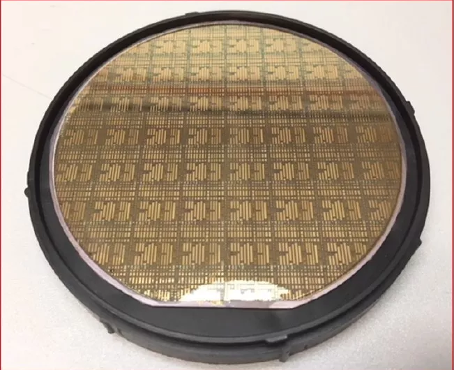
Figure 1: 4-inch diamond-based GaN wafer
GoDi HEMT devices developed and reported in the past have demonstrated excellent thermal and RF performance, but most work is done using small wafers (less than 4 inches). With the help of RFHIC's foundry partners, the fully automated 4-inch GoDiHEMT can now be manufactured. Using the standard SiC-based GaN process flow, the GaN HEMT process can be implemented with minimal process modifications. Since the GoDi HEMT wafer is very thin (about 120 μm thick), special carrier bonding techniques that can withstand various processes must be developed.
Since diamond is the hardest natural material, it is not possible to perform scribing and drilling using standard inserts or etching processes. RFHIC therefore conducted research using laser scribing and drilling. RFHIC successfully used laser drilling to achieve a 60 micron wide slot. RFHIC is also researching and developing a new plasma etch process that significantly enhances the drilling process.
Currently, 4-inch wafers are in the final stages of processing and will receive measurements in June 2018. Subsequent articles will report the detailed results of these research efforts.
references
1. F. Ejeckam, D. Francis, F. Faili, DJTwitchen, B. Bolliger, J. Felbinger and D. Babic, “S2-T1: GaN on Diamond: ABrief History,†Lester Eastman Conference on High Performance Devices, August 5-7 2014, DOI: 10.1109/LEC.2014.6951556. INSPEC Accession Number.
2. M. Wu, D. Hou and WS Lee, “Fabrication of 4-in. GaN/Diamond HEMT in a Compound Semiconductor Foundry,†CS Mantech2018, Austin, Texas.
Efficient heat-dissipating diamond-based GaN power amplifier for satellite communications
Felix Ejeckam, Ty Mitchell, Kris Kong and Paul Saunier, Akash Systems Inc., San Francisco, Calif.
State-of-the-art commercial satellites transmit data to the Earth at rates of 100 to 200 Mbps; some advanced large satellites are ideally targeted at 1 to 4 Gbps. These data rates are basically subject to the RF power amplifier of the transmitter. Akash is building its first small satellite system (12U) with an estimated downlink data rate of 14 Gbps. The next demonstration will achieve data rates in excess of 100 Gbps. The ultimate technical goal is to achieve a downlink data rate of 1 Tbps on medium-sized satellites using diamond-based GaN RF power amplifiers.
Diamond-based GaN
Aklix Systems co-founder Felix Ejeckam invented the diamond-based GaN1 in 2003, effectively extracting heat from the hottest locations in GaN transistors. The basic concept is that cooler GaN amplifiers can make systems more energy efficient and less wasteful. On a diamond-based GaN wafer, a GaN channel or epitaxial layer is stripped from its original Si substrate and bonded to a CVD diamond substrate through a 35 nm SiN interfacial layer. This nanoscale 200 ° C GaN channel combined with the thermally conductive industrial material CVD diamond greatly reduces the temperature rise between the amplifier substrate and the channel. Figure 2 shows the process flow for fabricating GaN on a diamond wafer. Over the years, several research institutes have quantified the above-mentioned thermal improvements2. The GaN on the SiHEMT wafer is bonded to the temporary Si carrier. The original Si substrate was etched away, and then diamond was deposited by CVD of a 35 nm interfacial layer under the GaN. Finally, the temporary Si carrier is etched away. The final diamond-based GaN wafer is then processed into a HEMT or MMIC array.
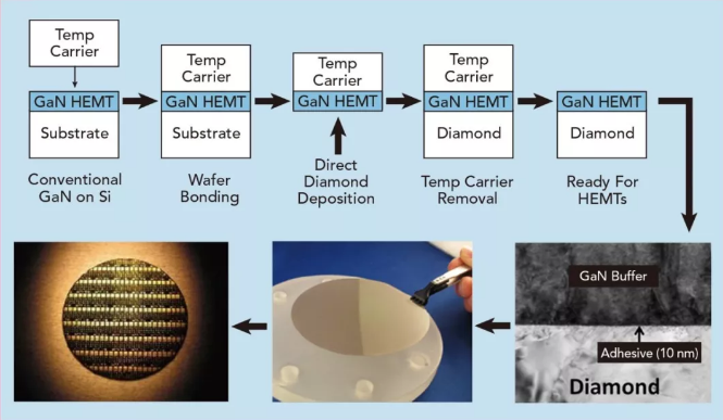
Figure 2: Diamond-based GaN process
    System impact
Compared to SiC-based GaN, if the temperature rise of the GaN MMIC can be reduced by 40% to 50%, a larger power density 3 can be obtained in a smaller volume. Power is a direct parameter in the satellite downlink data rate budget; if there is more power, more information can be transmitted. Diamond-based GaN can relax cooling requirements in a very compact space because ambient temperatures can rise higher than typical SiC power amplifier systems without compromising performance or reliability. The reduction in cooling means also means weight and size reduction, which is also a key factor in the cost of launching a satellite system into orbit.
performance
Akash designers recently demonstrated high-performance diamond-based GaN transistors (ie, simplified power amplifiers) on the K-band with 60% efficiency (PAE) at 20 GHz (see Figure 3). In another work performed by DARPA and conducted by a group of researchers at Georgia Tech, Stanford University, UCLA, and Element Six, the temperature of diamond-based GaN devices compared to the same devices for SiC-based GaN The temperature change from the GaN channel to the bottom of the substrate is reduced by 80 °C. The wafer used in this work is the same diamond-based GaN process used by Akash Systems.
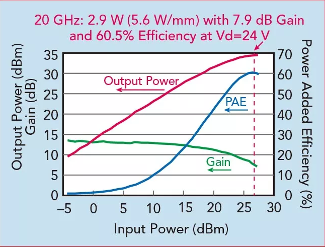
Figure 3: A 2.9 W (5.6 W/mm) HEMT swatch can achieve 61% efficiency with a gain of 7.9 dB. The bias voltage is 24V.
Figure 4 shows the temperature distribution from the center to the edge of the 10-fin HEMT for various types of GaN on a diamond wafer. Akash Systems uses a "gradient diamond with low thermal boundary resistance (TBR)" process to implement diamond-based GaN wafers (green). This curve records the peak temperature (first peak) at 152 °C. At the same location, the temperature of the SiC-based GaN device was 232 °C2.
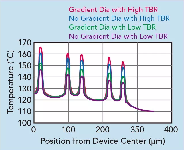
Figure 4: The graph shows the temperature distribution from the center to the edge of the 10-fin HEMT for various types of GaN on a diamond wafer.
Akash Systems plans to launch a LEO orbit 24 kg 12 U (36 cm x 24 cm x 23 cm) satellite system in 2019 that will include a 20 watt radio transmitter based on a diamond-based GaN power amplifier. The system will achieve a milestone 14 Gbps data rate, which is unique for satellite systems of this size.
references:
1. F. Ejeckam, D. Francis, F. Faili, DJ Twitchen, B. Bolliger, J. Felbinger and D. Babic, “S2-T1: GaN on Diamond: A Brief History,†Lester Eastman Conference on High Performance Devices, August 5–7 2014, DOI: 10.1109/LEC.2014.6951556. INSPEC Accession Number: 14775316.
2. L.Yates, A. Sood, Z. Cheng, T. Bougher, K. Malcom, J. Cho, M. Asheghi, K. Goodson, M. Goorsky, F. Faili, DJ Twitchen and S. Graham, “ Characterization of the Thermal Conductivity of CVD Diamond for GaN on Diamond Devices,†CompoundSemiconductor Integrated Circuit Symposium (CSICS) 2016 IEEE, pp. 1–4.
3. GDVia, JG Felbinger, J. Blevins, K. Chabak, G. Jessen, J. Gillespie, R. Fitch, A. Crespo, K. Sutherlin, B. Poling, S. Tetlak, R. Gilbert, T. Cooper , R.Baranyai, JW Pomeroy, M. Kuball, JJ Maurer and A. Bar-Cohen, “Wafer-ScaleGaN HEMT Performance Enhancement by Diamond Substrate Integration,†10th International Conference on Nitride Semiconductors, August 25-30, 2013, Washington, DC
High power diamond passive device
Ultra-small high power diamond RF resistor
Smiths Interconnect, Stuart, Fla.
In the past few decades, beryllium oxide (BeO) and aluminum nitride (AlN) have become the preferred substrate materials for high power RF resistors. These ceramic materials have high thermal conductivity and are sufficient for many applications; however, BeO and AlN substrates are often faced as designers face many SWaP-C (size, weight, power, cost) challenges while pursuing higher frequencies. Not suitable. In search of alternative technologies, RF engineers have turned to CVD diamond-based components to meet these needs.
CVD diamond is a single crystal carbon substrate material produced using a chemical vapor deposition process. Structurally, the Type 2 synthetic CVD diamond substrate, like natural diamond, can be processed into a circuit using a similar process to conventional RF substrate materials. A new development in Smiths Interconnect's CVD diamond film by sputtering tantalum nitride (TaN) on a CVD diamond substrate, resulting in a series of ultra-small, high-performance resistors, matchers and attenuators called diamond RF resistors (Diamond RF Resistives). Conductor materials are also sputtered onto the CVD diamond to form eutectic solder and wire bond pads, making these circuits easy to implement in a variety of mounting methods such as surface mount, chip bonding, and flanges.
A capacitance is created between the film material and the ground plane below the chip. Due to the direct correlation between substrate size and capacitance, typical CVD diamond thin film resistors consume up to eight times the area occupied by the same heat (see Figure 5). In addition, due to the relationship between capacitance levels and high power/high frequency performance, components fabricated using this material not only exhibit high power handling capability at higher frequencies per square millimeter, but also exhibit lower parasitic performance, ie Better isolation. For example, a single 0402 resistor fabricated on a CVD diamond substrate can consume 20 W of continuous wave and 200 W of power.

Figure 5: Diamond resistor.
Applications currently benefiting from this technology include advanced Wilkinson splitters/combiners, isolators, dual junction circulators/duplexers, and amplifier feedback networks. As a key element of space systems, radar and wireless infrastructure continue to drive performance improvements in passive resistors. In the next few years, Smiths Interconnect will continue to provide engineers with new diamond resistors based on CVD diamond substrates and SWaP-C solutions in all aspects of RF microwave systems.
Chemical vapor deposition diamond passive device
Res-Net Microwave, Clearwater, Fla.
Diamond synthesized by chemical vapor deposition has excellent thermal conductivity, which is three to four times that of copper. In addition, the low dielectric constant of chemical vapor deposited diamond makes it an excellent RF dielectric material for high frequency and high power applications. A power density comparison of chemical vapor deposited diamond and a standard ceramic substrate is given in Figure 6.
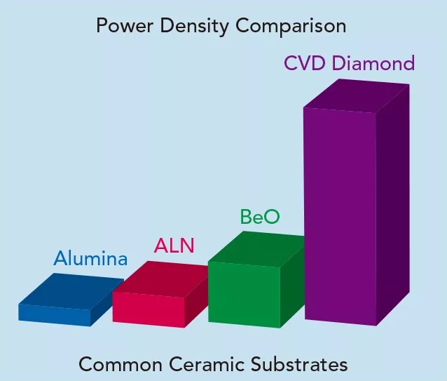
Figure 6: Power density comparison of chemical vapor deposited diamond and standard ceramic substrates.
The mechanical and electrical properties of chemical vapor deposited diamonds are well suited for making passive components such as resistors, loads and attenuators. Using chemical vapor deposition materials and off-the-shelf thin film processing technologies, these passive components can withstand the most challenging space environments. Therefore, these devices are used in many aerospace, military, and commercial applications.
The high thermal conductivity of chemical vapor deposition materials makes it possible to design small chips that can operate above 40 GHz and maintain continuous power consumption of more than 10 watts. In addition, for continuous wave applications, these passive components are also well suited for pulsed power applications. Res-Net manufactures diamond resistors, loads and attenuators. The sample resistors range in frequency from DC to 30 GHz, with a maximum power of 20 watts from DC to 30 GHz and a maximum power of 150 watts from DC to 18 GHz. The load range covers DC to 25 GHz, with a maximum power of 300 watts from DC to 16 GHz and a maximum power of 50 watts from DC to 25 GHz.
Diamond-based package
Aluminum-diamond metal based heat sink for gallium nitride devices
Kevin Loutfy, Nano Materials International Corp., Tucson, Ariz.
High-power RF and microwave transistors have long used various high thermal conductivity materials as substrate materials and heat carriers, including copper, copper-tungsten (200W/mK), copper-molybdenum (250W/mK) with thermal conductivity of 400W/mK. Copper-molybdenum-copper (350W/mK). For GaN devices, silicon carbide with a thermal conductivity of up to 400 W/mK is the substrate material for most high performance devices.
However, industrial grade synthetic diamonds have much higher thermal conductivity, ranging from 1200 W/mK to 2000 W/mK, which results in more heat being removed than any other material. In recent years, GaN device manufacturers have become increasingly interested in the significantly improved performance of gallium nitride discrete devices and MMIC devices as substrates and heat sinks. At present, there are not many devices using gallium nitride on diamond substrates, but the application of aluminum alloy-diamond metal matrix composites (MMC) produced by Nanomaterials International Corporation (NMIC) on various kinds of metal matrix composites. More and more extensive (Figure 7).
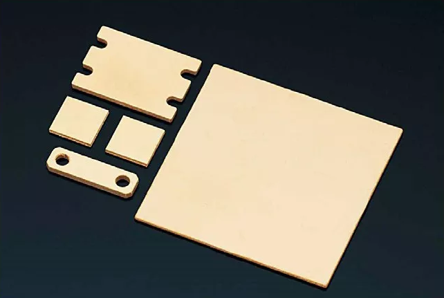
Figure 7: Aluminum-diamond MMC of different sizes.
The aluminum-diamond MMC heat sink is located underneath the mold or package and can be used regardless of whether the substrate material has a thermal conductivity of approximately 500 W/mK. Aluminum-diamond can function effectively in the press-bonding process, and its output is equivalent to or even superior to conventional heat sink materials. NMIC's aluminum-diamond composites use an aluminum alloy composition that penetrates into industrial grade diamond particle packages.
Diamond provides excellent thermal conductivity, aluminum provides structural and CTE distribution, and a very smooth surface with a silicon carbide stack connection surface at the top and bottom. The process flow for NMIC to produce aluminum-diamond composites is shown in Figure 8. The aluminum-diamond plate produced by the infiltration process, called the “motherboardâ€, cuts multiple parts from the mother board and optimizes the size with aluminum-diamond composites to meet the dimensional requirements of the parts, which reduces the cutting process of the mother board. Waste generated in the process. These parts are then nickel plated and gold plated to produce the final product. There are certain challenges in the development process that are related to the interface between the two materials. To solve this problem, NMIC proposed a technique for converting the surface of diamond into silicon carbide, a technology that has been patented by the company.
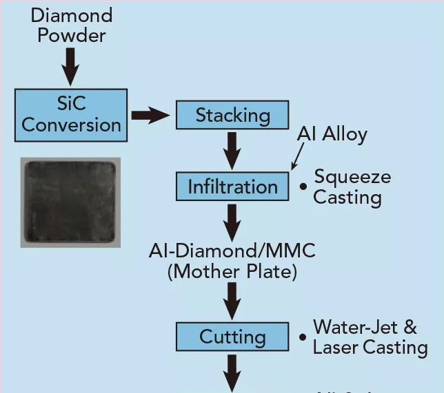
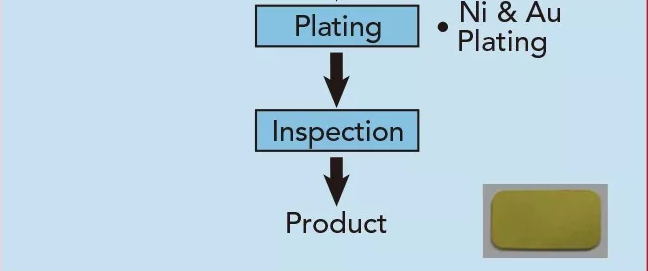
Figure 8: Production process of NMIC aluminum-diamond MMC.
In the past few years, this production process has become very distinctive. Aluminum-diamond composites are cost-effective and can be used in large sizes such as 45mm x 45mm, much larger than other diamond-based alternatives. The use of alternatives is limited by their size or thickness. Customers can use this composite in both hermetically sealed and unsealed packages for high reliability and space-level applications, all of which have stringent thermal cycling requirements.
In addition to high thermal conductivity, a stable CTE is also essential for a material that is attached to a transistor package. The CTE of aluminum-diamond is equal to the CTE of other engineering materials, but in the case of large size, the stability of aluminum-diamond makes it stand out, its CTE is 6.5-7.5ppm/K, close to gallium nitride.
In just a few years, improvements in aluminum-diamond composites have turned this technology into a technology that can replace other heat sinking materials. It takes advantage of the inherent high thermal conductivity of diamonds while also producing and providing better CTE performance than diamonds alone.
Diamond-silver composite package for GaN space applications
Richard Mumford, International Editor, Microwave Journal
As part of the EU Framework Programme 7, the advanced GaN packaging project from October 1, 2010 to March 31, 2012 is aimed at space applications, enabling Europe to maintain a strong position in the highly competitive aerospace industry. . The University of Bristol, Plamsee SE, United Monolithic Semiconductor and Thales Alenia Space highlighted the research on diamond-silver substrate materials1. A novel GaN electronic device packaging scheme is proposed for efficient extraction of heat required for high-power devices. The effect of diamond-silver composites as package substrates on self-heating of GaN devices is demonstrated for the first time.
A diamond-silver composite composed of diamond particles in a silver alloy matrix has an excellent thermal conductivity of up to 650 W/mK at room temperature, and the CTE is close to that of a semiconductor material, which is significantly greater than the thermal conductivity of a conventional encapsulating material such as CuW.
In this study, micro-Raman thermography measurements were performed on an AlGaN/GaN multi-finger HEMT (18-finger power board) to determine device temperatures at different power levels. The device was attached to a diamond-silver composite and a CuW substrate using standard AuSn solder. To evaluate the difference in thermal management efficiency between the two materials, Figure 9 shows the temperature at which the device center finger is Raman measured at different power values. That is, the peak temperature of the device rises while the temperature of the substrate behind it remains at 25 degrees Celsius.
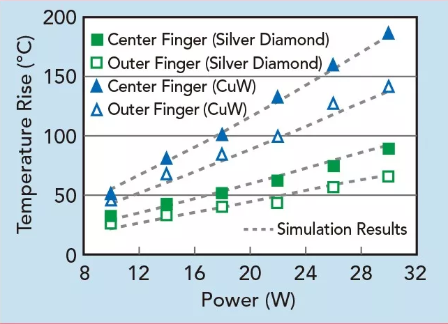
Figure 9: The peak temperature rise of the center interdigital finger as a function of the dissipated power when the AlGaN/GaN HEMT device (18 interdigital power board) is soldered to the diamond-silver composite and CuW substrate.
The peak temperature of a device mounted on a diamond-silver composite substrate is approximately half of the peak temperature of the device mounted on the CuW substrate, especially at high power, which is the standard for device operation. The temperature of the outer fingers also has the same trend. However, due to the crosstalk effect, the temperature of the center interdigital finger is higher.
In addition, there are significant improvements from the point of view of heat extraction, which have significant benefits for equipment reliability and system requirements. The device's three-dimensional finite element model was built for simulation and compared to experimental data. The simulation results agree well with the experimental results. Figure 10 shows the diamond-silver temperature distribution across the device as compared to the temperature profile on the CuW substrate. Similarly, in diamond-silver composited equipment, the temperature is significantly reduced.
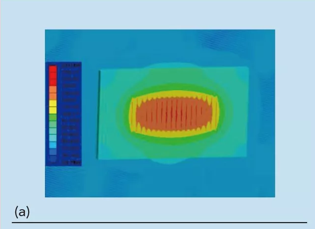
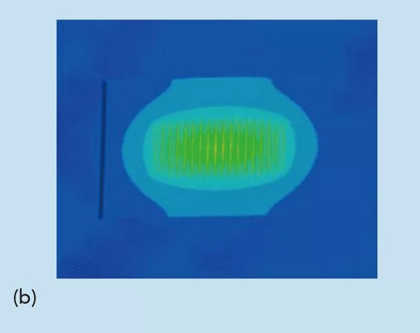
Figure 10: Temperature distribution of an AlGaN/GaN HEMT (18 interdigital power board) with a power dissipation of 30W. (a) a device soldered on a CuW substrate; (b) a device 1 soldered on a diamond composite substrate.
The final report of the project said: "L-band HPA has achieved the most advanced results, reflecting the strong impact of substrate materials on RF power modules. Up to 65% PAE and 180W RF power can be obtained in the L-band without adjustment A power module using a diamond-silver substrate material. For a similar design of the CuW standard micropackage, the gain of the PAE is approximately 10 points."
references
1.M. Faqir, T. Batten, T. Mrotzek, S. Knippscheer, L. Chalumeau, M. Massiot, M. Buchta, J. Thorpe, H. Blanck, S. Rochette, O. Vendier and M. Kuball, "NovelPackaging Solutions for GaN Power Electronics: Silver-Diamond Composite Packages," CS MANTECH Conference, May 2010.
Measuring Tape MID certification; ISO9001 certification;
1. Measuring tape Case: First-grade new ABS plastics: Bright, odorless.
2. Graduation: British-metric; metric; British; Luban etc.
3.Measuring tape Blade: steel,white and yellow colors,matt and shiny or chromed
4. Hook: Magnetic or common (it depends on custom request) the hook is flexible
5. Rivets: 3or 2 rivets hook reduces risk of breakage; the rivet can be fastened to a proper
position
6. Belt: The belt is made with Nylon for more handy and durable
7. Measuring tape Size: 1m/3ft-10m/33ft
Free Samples
We will offer you free sample within 5 working days after your comfirmation of details and
invoice.
Quality Guarantee
We will check the products strictly one by one before arranging the shippment.
Price Discount
We will give discount to the long term business partners or the big order.
Customized Service
We can offer the OEM service based on clients' requirements such as the color,label or the
package,etc.
Measuring Tape
*Impact resistant rubberized case;
*Heat-treated spring provides long life and smooth blade rewind;
*Strong belt clip
Steel Measuring Tape,Long Steel Measuring Tape,Long Tape Measure,Steel Tape Measure
Oukelong Tools Co.,Ltd , https://www.oukelongtape.com